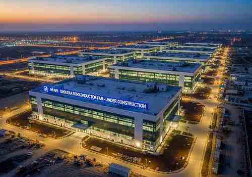
Overview
The country has been granted a Special Economic Zone (SEZ) by the Government of India to have the first semiconductor fabrication plant at Dholera. The project headed by Tata Semiconductor Manufacturing Private Ltd is a significant move towards establishing a domestic chip manufacturing ecosystem and minimize dependence on imports.
Project Size and Investment.
The fabrication plant will have an area of 66.16 hectares and will cost about 91,000 crore. It is projected to create approximately 21,000 jobs, and is one of the biggest high-technology manufacturing projects in India. The Department of Commerce has issued a SEZ notification which is indicative of a vigorous drive towards advanced industrial infrastructure.
Policy Reforms that will allow growth.
The consent is based on major modifications of the SEZ regulations in 2025. Land requirement in semiconductor units was also brought down to 10 hectares instead of 50 hectares making it easier to access by investors. These reforms form the wider policy agenda to entice international and national semiconductor actors.
Emerging Semiconductor Ecosystem
Dholera project is supported by other approved proposals. Micron Semiconductor Technology India Ltd is going to invest 13, 000 crores, and Kaynes Semiconductor Ltd and CG Semi Ltd are also targeting assembly, testing and packaging. These projects are indicative of the creation of a full semiconductor value chain in India.
Strategic and Economic Significance.
Semiconductors are essential for modern technologies such as AI, automobiles, and consumer electronics. The project increases the influence of India in the world supply chains and technological self-sufficiency. It fits the aim of decreasing the reliance on imports and increasing the high value production and innovation.
Exam-Focused Key Points
- First semiconductor fabrication SEZ at Dholera, Gujarat.
- Investment of ₹91,000 crore with 21,000 job potential.
- SEZ land requirement was decreased by half to 10 ha.
- Expansion of entire semiconductor ecosystem with packaging units.
- Favors supply chain resilience and technology self-dependence.
Practice Problems (answers)
Q1. In which is the location of the first semiconductor fabrication SEZ in India?
Answer: Dholera, Gujarat.
Q2. Who is the semiconductor fab leader?
Response: Tata Semiconductor Manufacturing Private Ltd.
Q3. Which policy modification facilitated Semiconductor SEZ development?
Response: Minimum land requirement cut by half to 10 hectares.
Q4. What is the strategic value of semiconductors?
Response: They are key elements of electronics and essential technology such as AI and cars.
Month: Current Affairs - Apr 16, 2026
Category: Economy | Science