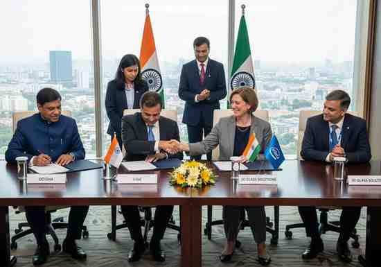
approval: August 2025.
Subsidiary implementing project: Heterogeneous Integration Packaging Solutions Private Limited (HIPSPL).
Investment by Intel, Lockheed Martin, Applied Materials: Approx. 11-13% equity each in 3DGS.
Key applications: AI, high-performance computing, 5G, defence, data centres, automotive, RF, photonics.
Related project: SiCSem compound semiconductor fabrication unit (groundbreaking June 2026).
Government framework: India Semiconductor Mission (ISM), Semicon India Programme.
Frequently Asked Questions (FAQ)
Q1. What is a semiconductor substrate?
A: A substrate is the base material that connects and supports semiconductor chips in electronic devices. It acts as a foundation for integrated circuits and helps chips communicate with each other.
Q2. Why is glass used instead of traditional materials for substrates?
A: Glass offers better thermal performance, higher integration density, prevents warping and allows more computing power. It is especially suitable for AI processors and heavy multi-chip architectures.
Q3. What is 3D Heterogeneous Integration (3DHI)?
A: 3DHI is an advanced chip packaging technology that stacks multiple components vertically in three dimensions. This allows faster, more energy-efficient chips used in AI, defence, and high-performance computing.
Q4. When will the facility start commercial production?
A: Commercial production is expected to begin by August 2028.
Q5. Is this the only semiconductor project coming up in Odisha?
A: No. Odisha is also hosting India's first commercial compound semiconductor fabrication unit by SiCSem Private Limited in collaboration with UK-based Clas-SiC Wafer Fab Ltd. Its groundbreaking is scheduled for June 2026.
Month: Current Affairs - May 30, 2026
Category: Intel3DGS